Source: 01 CUDA C Basics
The CUDA Stack
CUDA (Compute Unified Device Architecture) is NVIDIA’s parallel computing platform, and it is more than one thing. It bundles a programming model, the driver and runtime APIs, a compiler toolchain (nvcc, lowering to PTX and then SASS), and a library stack (cuBLAS, cuDNN, and the rest). CUDA C++ is the specific layer that extends C++ with device code; it is one part of the platform, not the whole of it. Since its 2007 release CUDA has become the de facto standard for deep-learning infrastructure, opening up the GPU as a general-purpose compute device (GPGPU) rather than a graphics-only one.
But when someone says “I use CUDA,” what exactly are they using? Running a model in PyTorch is CUDA. Writing a __global__ kernel by hand is also CUDA. The confusion comes from the fact that CUDA is a stack, not a single layer.
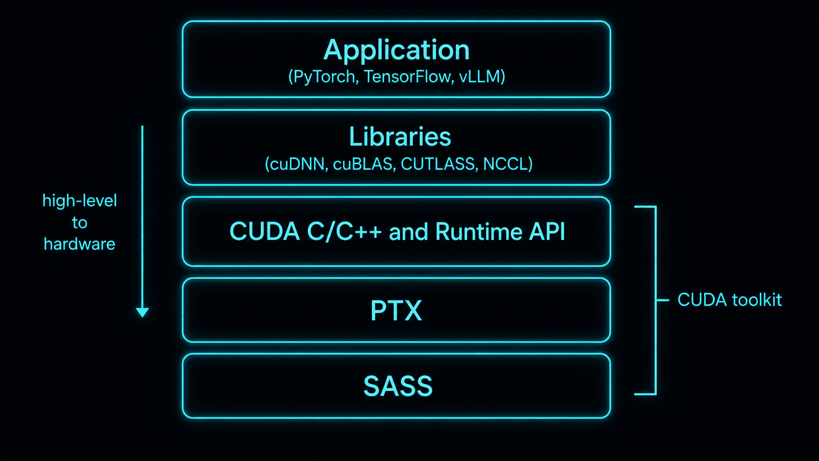
What people usually call “CUDA” spans layers 3-5 (CUDA C/C++, PTX, SASS).
| Layer | Role |
|---|---|
| CUDA C/C++ | The programming model you write directly. __global__, threadIdx, the Grid/Block/Thread abstraction |
| CUDA Runtime API | cudaMalloc, cudaMemcpy, kernel launches, etc. |
| nvcc | NVIDIA’s compiler that lowers the above to PTX / SASS |
| PTX | A virtual ISA. Handles forward compatibility across generations |
| SASS | The actual machine code, compiled for a specific GPU generation. Architecture-specific |
GPGPU
GPGPU (General-Purpose computing on GPU) means exactly what it says: using the GPU for compute beyond graphics. Before deep learning took off, the GPU was mostly a device for drawing polygons, but today any large-scale parallel numerical workload gets offloaded to it.
You’ve probably seen a CUDA - GPUs option in the settings of a video editor or an ML framework. That’s a setting for which GPU runs a program’s CUDA work: not for games, but for GPGPU workloads like video editing and machine learning.
The workloads where GPGPU shines share one trait: they repeat the same operation over huge amounts of data, independently. That structure maps cleanly onto the GPU’s SIMT (Single Instruction, Multiple Threads) execution model.
| Workload | Underlying operation |
|---|---|
| Video encoding / filters | Parallel numeric ops over a pixel matrix |
| DL training / inference | Tensor (multi-dim matrix) MatMul |
| Crypto mining | Massively parallel hash execution |
| Scientific simulation | Parallel updates of grid / particle systems |
| 3D rendering (Blender Cycles, etc.) | Per-ray parallel computation |
As an aside: one of the earliest cases of using a GPU to train a neural network was a 2004 paper by Korean researchers (Oh & Jung, “GPU implementation of neural networks,” Pattern Recognition). There was no CUDA back then, so they ran the network on shaders.
Heterogeneous Computing
Heterogeneous computing means different architectures (CPU and GPU) cooperating within a single system. The key idea in CUDA is not “run everything on the GPU.” Control flow and light logic stay on the CPU (Host); only the heavy compute (matrix and tensor ops) is offloaded to the GPU (Device).
Why the split? It comes down to two design philosophies. A CPU puts a few cores behind large caches and aggressive branch prediction to minimize latency on sequential code. A GPU does the opposite: it strips control logic and cache down and packs thousands of small cores to maximize throughput. So branchy, sequential code belongs on the CPU, while code that repeats the same operation thousands of times belongs on the GPU.
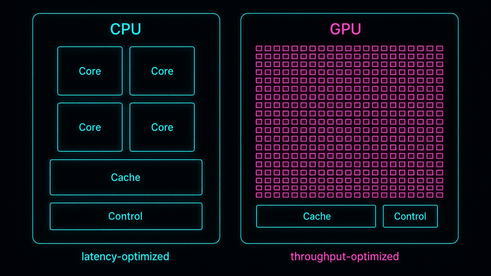 The CPU optimizes for latency with a few large cores; the GPU optimizes for throughput with thousands of small ones
Host-Device Data Flow
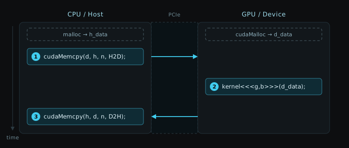
In the explicit-copy model this post uses, the CPU (Host) and GPU (Device) have separate physical memories: a variable allocated on the CPU is not visible to a kernel, so you move the data yourself. (cudaMallocManaged and Unified Memory, and integrated GPUs can share physical memory, so their placement rules differ; this post first establishes the explicit model.) Under it, every CUDA program goes through these three stages to bridge the memory gap.
- Host to Device (
cudaMemcpy)
cudaMemcpy(d_data, h_data, size, cudaMemcpyHostToDevice);
Copy the source data from CPU memory to GPU memory over the host-device interconnect, usually PCIe on a discrete GPU (NVLink only in topology-specific systems such as GH200).
- Execute Kernel (
<<<...>>>)
kernel<<<gridDim, blockDim>>>(d_data);
Run the parallel kernel on the GPU to do the actual work.
- Device to Host (
cudaMemcpy)
cudaMemcpy(h_result, d_result, size, cudaMemcpyDeviceToHost);
Bring the finished result back from GPU memory to CPU memory.
Why is this the single biggest optimization bottleneck? The bandwidth numbers make it obvious, as long as you keep the paths straight. The default host-to-device path for a discrete GPU is PCIe: PCIe Gen4 x16 is ~32 GB/s per direction (theoretical), Gen5 x16 ~64 GB/s. NVLink is far faster but topology-dependent; an H100’s NVLink is ~900 GB/s aggregate (bidirectional), and it applies to GPU-to-GPU over NVLink/NVSwitch or Grace-to-Hopper over the on-package NVLink-C2C link on GH200, not to a plain cudaMemcpy from system RAM, which still crosses PCIe. On-device HBM, meanwhile, is ~2.0 TB/s on an A100 SXM (HBM2e) and ~3.35 TB/s on an H100 SXM (HBM3). So on-device memory outruns the PCIe host link by roughly 30-100×, depending on the PCIe generation and the GPU.

That means each host-device round trip is expensive, which is why much of real-world optimization comes down to minimizing transfers. Pinned (page-locked) memory raises PCIe transfer bandwidth, cudaMemcpyAsync overlaps transfer with compute, and kernel fusion cuts the intermediate global-memory traffic and per-launch overhead between kernels; it removes a host round trip only in a pipeline that was staging intermediates back to the host. That’s the subject of the next post.
CUDA C Syntax and Kernels
What kind of “heavy computation” is worth paying that communication bottleneck? The example that most clearly shows the payoff in intro CUDA is vector addition. In c[i] = a[i] + b[i], each index is independent, so one thread per element is all you need. A textbook embarrassingly parallel problem.
To run this on the GPU, you first have to declare where each function runs and where it’s called from. CUDA C adds function qualifiers to C/C++ for exactly this.
| Qualifier | Runs on | Called from | Notes |
|---|---|---|---|
__global__ | Device (GPU) | Host (CPU) | The kernel that runs on the GPU. Must return void because the launch is asynchronous |
__device__ | Device (GPU) | Device (GPU) | A helper callable only from within the GPU |
__host__ | Host (CPU) | Host (CPU) | An ordinary C/C++ function (the default, can be omitted). Any unqualified function is __host__ |
The reason a __global__ kernel only returns void is the execution model. A kernel launch is asynchronous, so the CPU that called kernel<<<...>>>() does not wait for it to finish; it moves straight to the next line. There is no synchronous path to return a value on. If you need the result, you wait for completion with cudaMemcpy (an implicit sync) or cudaDeviceSynchronize, then read it back from device memory.
The nvcc Compilation Pipeline
A single .cu file can freely mix CPU code (main) and GPU code (__global__). NVIDIA’s compiler nvcc scans the source and splits the two apart.
Digging into the pipeline: host code is handed to a system C++ compiler (GCC, MSVC, etc.) as-is. Device code is lowered in two steps. First cicc (NVVM/LLVM-based) turns C++ into PTX, then ptxas compiles that PTX into SASS for a specific architecture. The final binary (a fatbin) usually embeds SASS for a few named architectures plus one forward-compatible PTX version. SASS is binary-compatible forward within a single major compute capability (sm_80 code also runs on sm_86 and sm_89, all major 8) but never across a major bump (sm_80 will not run on sm_90). So a next-major-generation GPU runs your binary only if it carries the forward-compatible PTX, which the driver JIT-compiles to SASS at load time. Build SASS alone with no PTX (as -arch=native does, since it emits SASS only), and the first next-major GPU it meets fails to load it. This is why PTX is called a “virtual ISA,” and why the -gencode arch=...,code=... flag controls both which architectures get pre-built SASS and whether PTX is carried along.
Rather than describe it, open it up. Dumping the add kernel with nvcc -arch=sm_80 -ptx vector_add.cu gives PTX whose core is:
mad.lo.s32    %r1, %r3, %r4, %r5;  // thread index i
setp.ge.s32   %p1, %r1, %r2;       // i >= N ?
@%p1 bra      $L__BB0_2;           // out of range -> skip
...
ld.global.f32 %f1, [%rd8];         // b[i]
ld.global.f32 %f2, [%rd6];         // a[i]
add.f32       %f3, %f2, %f1;       // a[i] + b[i]
st.global.f32 [%rd10], %f3;        // c[i] = ...
You can see exactly how the single C line (c[i] = a[i] + b[i]) lowers. The index math folds into one mad.lo.s32, a 32-bit integer multiply-add for the address calculation, not an FP32 fused-multiply-add, if (i < N) becomes setp plus a predicated branch (@%p1 bra), and the actual work is two global loads, one FP32 add, and one global store. The “12 bytes and 1 FLOP per element” from the roofline analysis later is exactly these four lines. From here ptxas lowers this PTX to architecture-specific SASS, which you can inspect with cuobjdump -sass.
Thread and Block Limits
- Threads per block max out at 1024. You’re free to split across dimensions (
dim3), but if the product exceeds 1024 the launch fails withcudaErrorInvalidConfiguration.dim3(32, 32, 1)(=1024) passes;dim3(32, 32, 2)(=2048) dies. There’s also a separate cap of 64 on the z-axis that’s easy to forget. - Grids are far more generous: 2³¹-1 on the x-axis and 65535 each on y/z. You won’t hit these with any reasonable dataset.
- Shared memory has three numbers people conflate. The static per-block limit is 48 KB (a compatibility default, the same on every architecture). The opt-in dynamic per-block maximum is higher and requested with
cudaFuncSetAttribute(kernel, cudaFuncAttributeMaxDynamicSharedMemorySize, bytes): ~163 KB on A100 (cc 8.0), ~227 KB on H100 (cc 9.0). Both are carved out of the SM’s combined L1/shared-memory capacity, 192 KB on A100, 256 KB on H100, which hardware partitions between L1 cache and shared memory.
These numbers aren’t arbitrary; they come from the hardware. A block runs to completion on exactly one SM (Streaming Multiprocessor) and is never split across SMs, and the SM schedules that block in units of warps. So the 1024-thread cap per block is 32 warps. On top of that, an SM has a finite register file: recent architectures have 65,536 32-bit registers per SM, shared among every thread resident on that SM. If a thread uses a lot of registers, fewer threads can be resident at once. That is exactly the occupancy story in the next section.
Warps and SIMT Execution
The GPU executes threads in groups called warps. A warp is 32 threads, a number fixed across every generation of NVIDIA GPU that developers cannot change.
Why does the warp matter for performance? The warp is the unit a scheduler issues: on a given cycle a warp scheduler issues one instruction for the active mask of its 32 lanes (SIMT). When lanes take different sides of an if/else (warp divergence), those paths serialize, the hardware runs one path with the other lanes masked off, then the other. Since Volta (cc 7.0), independent thread scheduling gives every thread its own program counter, so divergent lanes may interleave and there is no guaranteed immediate reconvergence at the branch’s post-dominator; call __syncwarp() when you need the lanes stepping together again. Either way, a partly-filled final warp still occupies a full 32-lane issue slot, which is why a thread count that is not a multiple of 32 wastes lanes.
For example, a block of 100 threads makes the GPU reserve scheduling slots for 4 warps (128 threads) while only 100 actually work. The remaining 28 slots sit idle, so utilization drops to 100/128 ≈ 78%. You throw away about 22% before you even start.
That is why block sizes are usually 128, 256, or 512, but the real decision criterion is occupancy: active warps resident on an SM divided by the SM’s maximum, which is itself architecture-dependent: 64 warps on A100 (cc 8.0) and H100 (cc 9.0), 48 on consumer Ampere (cc 8.6) and Ada (cc 8.9). The other per-SM resources are fixed the same way. On cc 8.0: up to 2048 resident threads, 32 resident blocks, 65,536 registers, and up to 164 KB of shared memory (228 KB on H100). Whichever runs out first sets the occupancy.
The reason occupancy matters is that the GPU’s performance model comes down to latency hiding. A global memory access takes hundreds of cycles (roughly 400 to 800), while an FP operation finishes in 4 to 6. When a warp stalls on a global load, the SM’s warp scheduler switches in the same cycle to another warp that is ready to run. That switch is free because the registers of every warp resident on the SM live in the register file at once, so there is no context to save and restore as there is on a CPU. The more warps are resident, the higher the chance that some warp is ready while others wait on memory. Raising occupancy is not about keeping cores busy; it is about hiding memory latency.
The number of blocks that can be resident on one SM is the minimum over four independent limits, threads, hardware block slots, registers, and shared memory, and occupancy follows from it:
$$ B_{\text{res}} = \min\!\left( \left\lfloor \tfrac{T_{\text{SM}}}{T_{\text{block}}} \right\rfloor,\; B_{\text{SM}}^{\max},\; \left\lfloor \tfrac{R_{\text{SM}}}{R_{\text{thread}}\, T_{\text{block}}} \right\rfloor,\; \left\lfloor \tfrac{S_{\text{SM}}}{S_{\text{block}}} \right\rfloor \right) $$$$ \text{active warps} = B_{\text{res}} \left\lceil \tfrac{T_{\text{block}}}{32} \right\rceil, \qquad \text{occupancy} = \frac{\text{active warps}}{W_{\text{SM}}^{\max}} $$These per-SM limits are set by compute capability. On cc 8.0 (A100): $T_{\text{SM}}=2048$, $B_{\text{SM}}^{\max}=32$, $R_{\text{SM}}=65536$, $W_{\text{SM}}^{\max}=64$. Take $T_{\text{block}}=256$: the thread limit gives $\lfloor 2048/256 \rfloor = 8$ blocks, and registers bound it too, 8 resident blocks need $8 \cdot 256 \cdot R_{\text{thread}} \le 65536$, i.e. $R_{\text{thread}} \le 32$. Above 32 registers per thread, fewer blocks fit and occupancy falls. (Hardware allocates registers per warp at a fixed granularity, so the real cutoff is a little coarser than this bound.) One edge case the formula needs: a kernel that allocates no shared memory has $S_{\text{block}} = 0$, so the shared-memory term is dropped (read it as $+\infty$) and never binds. Vector add is exactly that case.
High occupancy is not the goal in itself; it is one lever for hiding memory latency. Once latency is already hidden, more occupancy buys nothing and can even hurt by shrinking the per-thread register budget. Instruction-level parallelism, achieved DRAM bandwidth, and cache behavior all matter alongside it. Measure rather than assume: sm__warps_active.avg.pct_of_peak_sustained_active in Nsight Compute reports achieved occupancy, which is what actually counts.
Memory Coalescing
How you read global memory (HBM) inside the kernel matters as much as the host-device transfer. The GPU coalesces the global memory requests issued by a warp’s 32 threads into hardware transactions.
On compute capability 6.0 and later (Pascal onward, including A100 and H100), the global memory transaction unit is a 32-byte sector. A warp reading 32 contiguous 4-byte words touches a 128-byte span, which is exactly four sectors. When a warp issues a global load, the hardware maps the 32 lane addresses to the sectors that cover them and moves those whole sectors. Let $S$ be the number of distinct 32-byte sectors a warp touches on one load. Bus efficiency is the bytes requested over the bytes actually moved:
$$ S = \bigl|\{\, \lfloor \text{addr}_{\text{lane}}/32 \rfloor \,\}\bigr|, \qquad \eta = \frac{\text{requested bytes}}{32\,S} $$Work the two ends for a warp loading 32 floats (requested $= 32 \times 4 = 128$ B):
- Contiguous and aligned: the 128 B spans exactly four sectors, $S = 4$, so $\eta = 128 / (32 \cdot 4) = 1$. The right description is four 32-byte sectors (a 128-byte contiguous span), fully used, not “one transaction.”
- Fully scattered: each lane lands in its own sector, $S = 32$, so $32 \cdot 32 = 1024$ B move for 128 B requested and $\eta = 128/1024 = 1/8$. For 4-byte elements the floor is $1/8$, not $1/32$; the old “$1/32$” assumes 128-byte transactions, which is not how sectored access works.
This is why vector addition is fast: i = blockIdx.x * blockDim.x + threadIdx.x makes adjacent lanes read adjacent addresses (a[0], a[1], a[2] …), so a warp hits four contiguous sectors and $\eta = 1$. Read it strided, like a[i * stride], and $\eta$ falls toward $1/8$ while the kernel slows in step. Nsight Compute measures it directly: l1tex__t_sectors_pipe_lsu_mem_global_op_ld.sum counts sectors moved and l1tex__t_requests_pipe_lsu_mem_global_op_ld.sum counts the load requests, so their ratio is the average sectors-per-request (ideal 4 for a full-warp 32-bit load, worst 32), which is the coalescing quality. The rule “map threads to the fastest-varying dimension (x)” is just keeping that ratio at its floor.
Block Independence
Threads within the same block share shared memory and synchronize with __syncthreads(), because they physically sit on the same SM.
Different blocks are different. What CUDA guarantees is that thread blocks in an ordinary kernel must be able to run independently in any order, with no general in-kernel barrier or ordering between arbitrary blocks, Block 7 may finish before Block 0. Blocks can still communicate indirectly through global memory and atomics, just with no ordering or visibility guarantee unless you impose one. When you truly need a device-wide barrier, the sanctioned options are a second kernel launch, a cooperative launch with Cooperative Groups grid.sync(), or (on Hopper) thread block clusters with distributed shared memory.
The reason is that the block-to-SM mapping is a hardware constraint. Threads in the same block share shared memory because it physically lives in that SM’s SRAM; blocks can’t talk to each other because they’re on different SMs with separate SRAM.
But this constraint is actually CUDA’s most important design decision. Because blocks are independent, the runtime can hand them out to whatever SMs are free, in any order. Whether a GPU has 20 SMs (a laptop chip) or 132 (an H100), the same kernel binary parallelizes across however many SMs are present. You change nothing, and a bigger GPU just runs faster. NVIDIA calls this transparent scalability. Giving up inter-block communication is the price paid for it, and it is why the Grid/Block/Thread software hierarchy lines up with the SM/warp/lane hardware, though, as the diagram below simplifies, that correspondence is one of scheduling, not a fixed one-to-one binding. A block is assigned to an SM and stays there; the SM issues that block’s threads 32 at a time as warps; and a “CUDA core” is a scalar execution unit (an ALU/FP lane) that runs one lane’s arithmetic on the cycle its warp issues. A thread is a software execution context, not a physical core it owns.
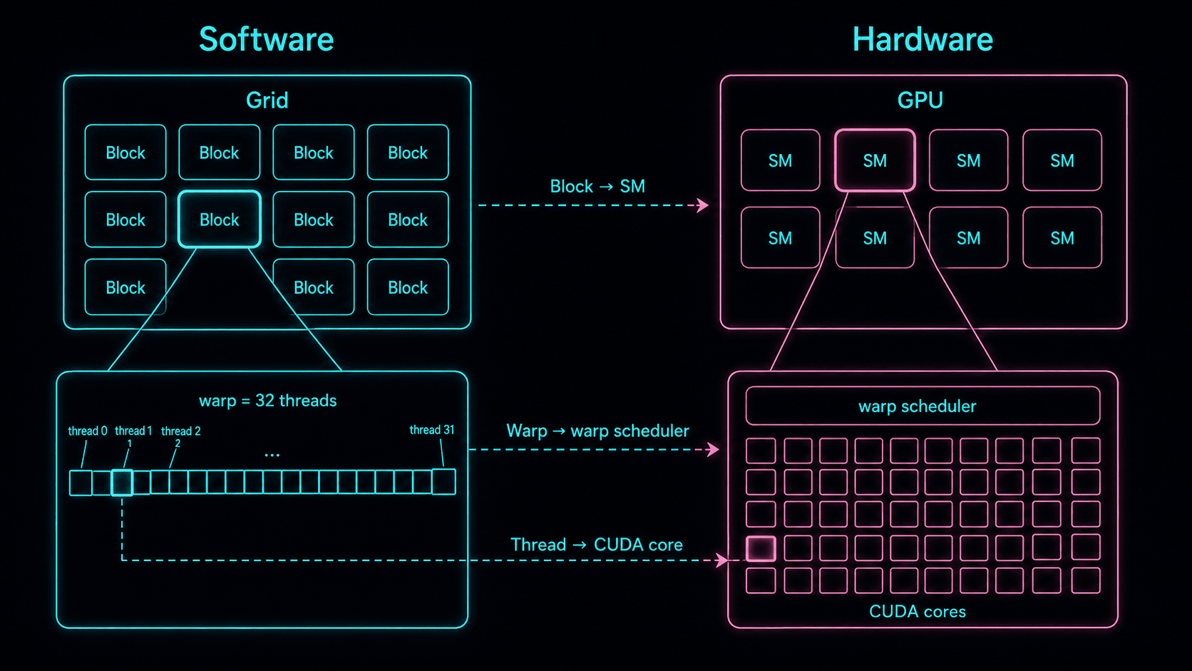 Grid/Block/Thread (software) scheduled onto GPU/SM/warp-scheduler/execution-units (hardware). A block is placed on an SM, threads issue 32 at a time as warps, and a CUDA core executes one lane’s arithmetic, a scheduling correspondence, not a fixed thread-to-core binding.
Here’s that hierarchy laid out by dimension:
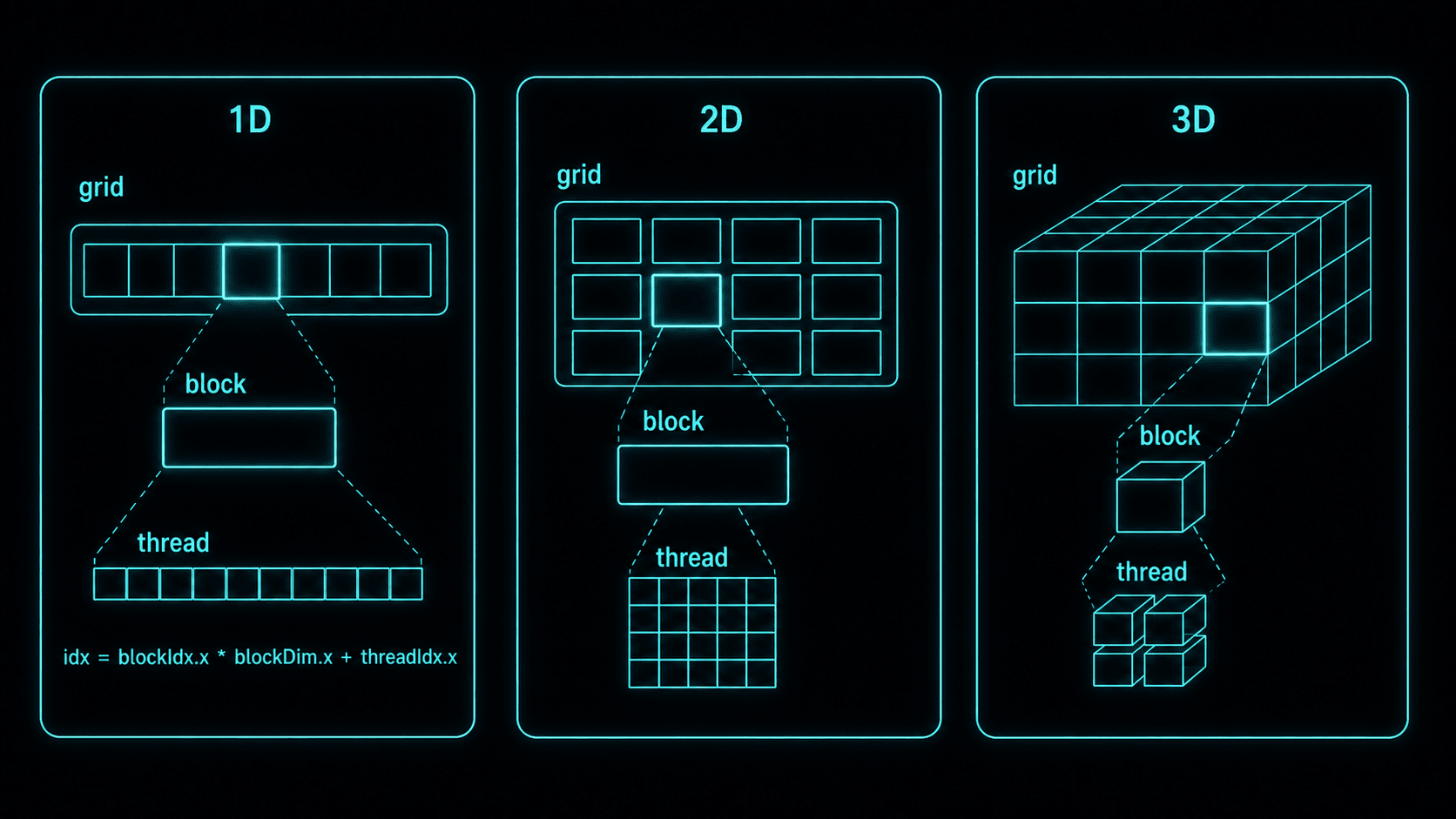 Layout by dimension. 1D
 kernel<<<4, 8>>> (32 threads), 2D kernel<<<dim3(2,2), dim3(4,4)>>>, 3D kernel<<<dim3(2,2,2), dim3(2,2,2)>>> (64 threads). The global index is blockIdx.x * blockDim.x + threadIdx.x
Execution Configuration: <<<>>>
Calling a __global__ function like a normal function is a compile error. You must use the triple chevron syntax.
mykernel<<<gridDim, blockDim>>>(args);
//        ^^^^^^^  ^^^^^^^^
//        number of blocks, threads per block
gridDim: how many blocks are in the gridblockDim: how many threads are in each block- Total threads =
gridDim × blockDim
The simplest example:
mykernel<<<1, 1>>>(); // 1 block, 1 thread → effectively sequential
To process N elements like in vector addition, you need N threads. The original video simplifies this to <<<N, 1>>>, but because of the warp efficiency above, 128 to 512 threads per block is more efficient in practice. Just size the grid by dividing N by the block size, rounding up.
int N = 10000;
int blockSize = 256;
int gridSize = (N + blockSize - 1) / blockSize;  // ceiling division
add<<<gridSize, blockSize>>>(a, b, c, N);
One more common idiom: instead of sizing the grid exactly to the data, you can fix the grid and have each thread process several elements, a grid-stride loop. Each thread steps by blockDim.x * gridDim.x, which decouples the launch config from the data size and stays safe when N exceeds the grid’s capacity.
__global__ void add(float* a, float* b, float* c, int N) {
    int stride = blockDim.x * gridDim.x;
    int i = blockIdx.x * blockDim.x + threadIdx.x;
    for (; i < N; i += stride)
        c[i] = a[i] + b[i];
}
Worked Example: Vector Add
Putting the pieces together (the 3-stage transfer, the qualifiers, the launch config) gives this. Save it as vector_add.cu and it compiles and runs as-is.
#include <cstdio>
#include <cstdlib>
#include <cmath>
#include <cuda_runtime.h>

__global__ void add(const float* a, const float* b,
                    float* c, int N) {
    int i = blockIdx.x * blockDim.x + threadIdx.x;
    if (i < N) c[i] = a[i] + b[i];   // skip out-of-range threads
}

int main() {
    const int N = 1 << 20;                 // ~1M elements
    const size_t bytes = N * sizeof(float);

    // 1) Host allocation + init
    float *h_a = (float*)malloc(bytes);
    float *h_b = (float*)malloc(bytes);
    float *h_c = (float*)malloc(bytes);
    for (int i = 0; i < N; i++) { h_a[i] = 1.0f; h_b[i] = 2.0f; }

    // 2) Device allocation
    float *d_a, *d_b, *d_c;
    cudaMalloc(&d_a, bytes);
    cudaMalloc(&d_b, bytes);
    cudaMalloc(&d_c, bytes);

    // 3) Host -> Device
    cudaMemcpy(d_a, h_a, bytes, cudaMemcpyHostToDevice);
    cudaMemcpy(d_b, h_b, bytes, cudaMemcpyHostToDevice);

    // 4) Launch (256 threads/block, grid by ceiling division)
    int blockSize = 256;
    int gridSize = (N + blockSize - 1) / blockSize;
    add<<<gridSize, blockSize>>>(d_a, d_b, d_c, N);

    // 5) Device -> Host (cudaMemcpy implicitly waits for the kernel)
    cudaMemcpy(h_c, d_c, bytes, cudaMemcpyDeviceToHost);

    // 6) Verify: 1.0 + 2.0 should be 3.0
    float maxErr = 0.0f;
    for (int i = 0; i < N; i++)
        maxErr = fmaxf(maxErr, fabsf(h_c[i] - 3.0f));
    printf("max error: %f\n", maxErr);

    // 7) Cleanup
    cudaFree(d_a); cudaFree(d_b); cudaFree(d_c);
    free(h_a); free(h_b); free(h_c);
    return 0;
}
Compile and run:
$ nvcc vector_add.cu -o vector_add
$ ./vector_add
max error: 0.000000
This single file contains everything from the earlier sections: the qualifier (__global__), the three transfers (cudaMemcpy three times), the launch config (<<<gridSize, blockSize>>>), and the bounds check (if (i < N)). One caveat: this code skips error handling for brevity. In real code you check the return value of every CUDA call and call cudaGetLastError() right after the launch, because a failed kernel launch fails silently.
Roofline: Bandwidth-Bound
Vector addition gets used as the example of “compute the GPU speeds up,” but an expert reads it the opposite way. This kernel barely does any FLOPs. Per element it moves 12 bytes (two loads for a and b, one store for c) and performs exactly one addition. That ratio is the arithmetic intensity.
$$ \begin{aligned} Q &= 2 \times 4\,\text{B} \;+\; 1 \times 4\,\text{B} = 12\,\text{B} \quad(\text{load } a,b\text{; store } c) \\ I &= \frac{W}{Q} = \frac{1\ \text{FLOP}}{12\ \text{B}} \approx 0.083\ \text{FLOP/B} \end{aligned} $$This value decides whether a kernel is compute-bound or memory-bound. The framework is the roofline model: the performance a kernel can reach is capped by the lower of its compute ceiling and its bandwidth ceiling.
$$P = \min\!\bigl(P_{\text{peak}},\ I \cdot \beta\bigr)$$The two ceilings meet at the ridge point $I^{*} = P_{\text{peak}} / \beta$. If $I$ sits left of it the kernel is memory-bound, right of it compute-bound. For an A100 (FP32 peak $P_{\text{peak}} \approx 19.5$ TFLOP/s, HBM $\beta \approx 2.0$ TB/s) the ridge point is
$$I^{*} = \frac{19.5 \times 10^{12}}{2.0 \times 10^{12}} \approx 9.75 \ \text{FLOP/byte}$$Vector addition’s $I = 0.083$ sits more than 100× to the left of that. It is entirely memory-bound, and its performance ceiling is
$$ \begin{aligned} P_{\text{vadd}} = I \cdot \beta &= \frac{1\ \text{FLOP}}{12\ \text{B}} \times 2.0\times10^{12}\ \text{B/s} \\ &= 1.67\times10^{11}\ \text{FLOP/s} \\ &\approx 166\ \text{GFLOP/s} \quad(0.85\%\text{ of }P_{\text{peak}}) \end{aligned} $$less than 1% of the A100’s FP32 peak. So vector addition demonstrates bandwidth and parallel indexing, not the GPU’s compute power. The operations that actually win on a GPU have high arithmetic intensity, like matrix multiplication, which reads data once and reuses it many times. Much of deep-learning kernel optimization is exactly this: raising data reuse to push $I$ to the right of the ridge point.
You can confirm the memory-bound verdict empirically instead of trusting the algebra. Time the kernel with cudaEvents and divide bytes moved by elapsed time for effective bandwidth; in Nsight Compute, dram__bytes.sum.per_second (or DRAM Throughput %) reports how close you got to $\beta$. A well-tuned vector add can approach a high fraction of peak HBM bandwidth (measure your own GPU for the number) and stays nowhere near peak FLOP/s, exactly what the roofline predicts.
The numbers inside <<< >>> map directly onto the GPU’s physical structure (SM, warp, block). Unlike other languages that hide the hardware, CUDA exposes it and puts performance in the developer’s hands. That’s both why you learn CUDA and why it’s hard.
References
- CUDA C++ Programming Guide: the primary source for the programming model, occupancy, and the memory hierarchy
- CUDA Compiler Driver NVCC: the compilation pipeline and
-gencode - Nsight Compute: profiling occupancy and limiting resources