Reference: Thomas L. Floyd, Digital Fundamentals, Pearson. Chapter 1, Introductory Concepts.
This course deals with circuits that process signals represented by the two values 0 and 1. The first half covers the rules of numbers and logic, such as number systems, logic gates and Boolean algebra, and the second half covers the smallest circuits that implement those rules, such as latches, flip-flops, registers and counters1. The material below corresponds to Sections 1.1 through 1.4 of the textbook and to lecture slides2 2 through 26. Chapter 1 defines only the inputs and outputs of each block, and later chapters build the circuits inside.
Analog and digital quantities
An analog quantity takes continuous values. The temperature over a day passes through every intermediate value between any two instants, so it is an analog quantity. A digital quantity takes only distinct discrete values, and in a digital circuit those values are 0 and 13.
To bring an analog quantity into a digital circuit, its value is read at fixed time intervals. Reading the value is sampling, and forcing each reading onto one of a fixed set of levels is quantization. In the figure below the cyan curve is the continuously varying temperature and the magenta dots are the samples read once per hour.
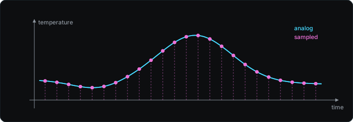
The textbook contrasts the two kinds of quantity with three systems.
| System | Signal processing |
|---|---|
| Public address system (microphone, amplifier, speaker) | Amplifies the audio waveform as it is. Analog from end to end |
| CD player | Reads digitally stored data and rebuilds an analog audio waveform with a DAC4 |
| Mechatronics (robotic arm) | Electronic controls decide digitally and an electromechanical interface moves the motors |
Transmitting a voice follows the same order. The analog voice is sampled into data, the data is sent, and the receiving side restores an analog waveform5. The converters that move between AC and DC among the charger, battery and motor of an electric vehicle6 are another case where both forms of signal are used in turn inside one device.
Logic levels
In a digital circuit 1 and 0 are defined as voltage ranges. HIGH (1) runs from $V_{H(min)}$ to $V_{H(max)}$, LOW (0) runs from $V_{L(min)}$ to $V_{L(max)}$, and the band between the two ranges is not interpreted as either value. When the voltage falls in that band the circuit does not guarantee a value.
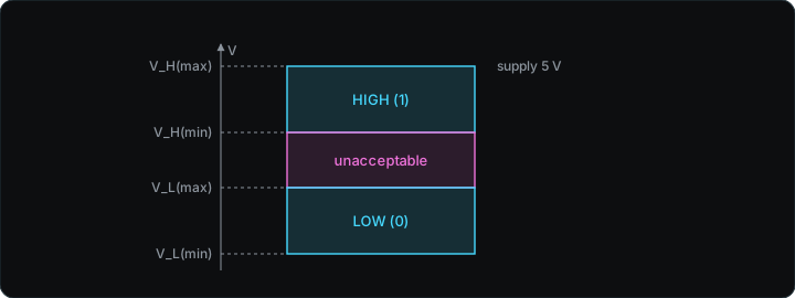
The upper limit of HIGH is the supply voltage applied to the circuit. The 74-series ICs7 used in the laboratory run with 5 V on pin 14, $V_{CC}$.
Pulses
A pulse is a single excursion from one level to the other and back. The instant of going from LOW to HIGH is the rising edge (leading edge) and the instant of going from HIGH to LOW is the falling edge (trailing edge). A pulse that starts from LOW is positive-going and a pulse that starts from HIGH is negative-going.
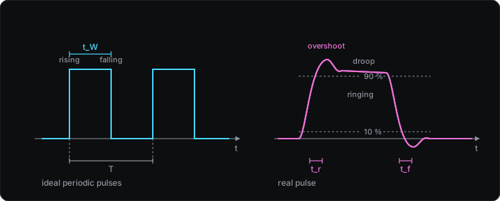
An ideal pulse changes voltage instantaneously at both edges. A real pulse takes time at each edge, and the textbook describes its characteristics in five terms.
| Term | Definition |
|---|---|
| Rise time $t_r$ | Time to go from 10 % to 90 % of the amplitude |
| Fall time $t_f$ | Time to go from 90 % to 10 % of the amplitude |
| Pulse width $t_W$ | Time between the 50 % points of the rising and falling edges |
| Overshoot, ringing | Passing the target level right after an edge and oscillating back to it |
| Droop | Gradual sag of the voltage during the HIGH interval |
When the period is on the order of 1 s, $t_r$ and $t_f$ are negligible compared with the period. When the clock reaches the GHz range and the period is on the order of ns, $t_r$ takes up a substantial part of the period and the waveform moves away from a square wave toward a triangle8. The theory in the textbook assumes ideal pulses.
Periodic waveforms, frequency and duty cycle
A periodic waveform repeats the same shape at a fixed time interval, and that interval is the period $T$. A nonperiodic waveform has no fixed repetition interval. The frequency $f$ is the number of repetitions in one second and its unit is Hz.
$$ f = \frac{1}{T}, \qquad T = \frac{1}{f} $$With $T = 0.1\ \mathrm{s}$ the frequency is $f = 10\ \mathrm{Hz}$, and with $f = 1\ \mathrm{GHz}$ the period is $T = 1\ \mathrm{ns}$9. The duty cycle is the fraction of one period during which the waveform is HIGH, that is the fraction taken by $t_W$.
$$ \text{duty cycle} = \frac{t_W}{T} \times 100\ \% $$The left side of the figure below is a periodic waveform made of ideal pulses with $T$ and $t_W$ marked. The right side is a single real pulse with the 10 % and 90 % lines used to measure $t_r$ and $t_f$.
The clock and timing diagrams
The clock is a pulse waveform with a constant period, and it sets the instants at which the other signals in a circuit may change value. One clock period is called the bit time. A data waveform represents one bit per bit time and does not change value within a bit time10. In the laboratory the clock comes from a function generator11 (an instrument that outputs a waveform of the frequency and amplitude entered on it).
A timing diagram draws several digital signals side by side on one time axis to show the state of each signal and the relative timing of their transitions. The figure below shows the clock and three inputs A, B and C over clock periods 1 through 8, with period 7, where all three inputs are HIGH, shaded.
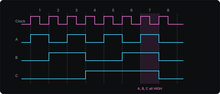
Reading (A, B, C) in each clock period gives the table below. With C as the most significant bit, periods 1 through 7 count upward in binary from 1 to 7.
| Period | 1 | 2 | 3 | 4 | 5 | 6 | 7 | 8 |
|---|---|---|---|---|---|---|---|---|
| A | 1 | 0 | 1 | 0 | 1 | 0 | 1 | 0 |
| B | 0 | 1 | 1 | 0 | 0 | 1 | 1 | 0 |
| C | 0 | 0 | 0 | 1 | 1 | 1 | 1 | 0 |
Each column of this table is an input combination for a logic gate. A gate produces a fixed output for each column, so the output waveform is updated with the same period as the clock12.
Serial and parallel transfer
Serial transfer sends bits one per bit time over a single data line. Sending 8 bits takes 8 bit times. Parallel transfer uses one line per bit and sends all bits at once in a single bit time13.
Basic logic functions
A logic gate is a circuit that produces a fixed output bit for each combination of input bits. NOT, AND and OR are the three basic functions, and every digital operation in later chapters is a combination of these three. The inputs are written $A$ and $B$ and the output $X$.
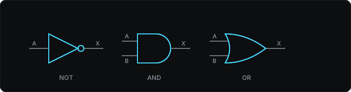
| Function | Operation | Truth table ($A\,B \to X$) |
|---|---|---|
| NOT | Inverts the input | $0 \to 1$, $1 \to 0$ |
| AND | 1 only when every input is 1 | $00 \to 0$, $01 \to 0$, $10 \to 0$, $11 \to 1$ |
| OR | 1 when at least one input is 1 | $00 \to 0$, $01 \to 1$, $10 \to 1$, $11 \to 1$ |
A truth table lists every possible input combination with its output, and with $n$ inputs it has $2^n$ rows. The small circle at the end of a symbol means inversion14. AND and OR differ only when the two inputs differ, and the function that outputs 1 exactly in that case is XOR15 (exclusive OR).
Logic function blocks
Section 1.4 of the textbook introduces blocks that group several gates into one function, described only by their inputs and outputs16.
| Block | Inputs | Outputs |
|---|---|---|
| Comparator | Binary numbers $A$, $B$ | Three lines $A > B$, $A = B$, $A < B$; only the line whose condition holds is HIGH |
| Adder | Binary numbers $A$, $B$ and carry input $C_{in}$ | Sum $\Sigma$ and carry output $C_{out}$ |
| Encoder | One HIGH line among many input lines | The binary code of that input’s number |
| Decoder | A binary code | The output pattern assigned to that code |
With $A = 2$ and $B = 5$ only the $A < B$ line of the comparator is HIGH. The adder’s $C_{out}$ is the 1 produced when the sum overflows one digit, and $C_{in}$ is the 1 carried up from the digit below17. An encoder turns the one key pressed on a calculator keypad into a binary code for storage, and a decoder takes that code and selects which bars of a 7-segment display18 to light. With 10 keys, $2^3 = 8 < 10 \le 16 = 2^4$, so the encoder needs 4 output lines.
Blocks that operate on the clock
Registers and counters are circuits whose stored value changes each time a clock pulse arrives. Unlike the blocks of the previous section, whose result appears as soon as the inputs are applied, time order is involved19.
| Block | Operation |
|---|---|
| Multiplexer (MUX) | Connects the one input line chosen by a select signal to a single output line |
| Demultiplexer (DEMUX) | Routes the received data to the one output line chosen by a select signal |
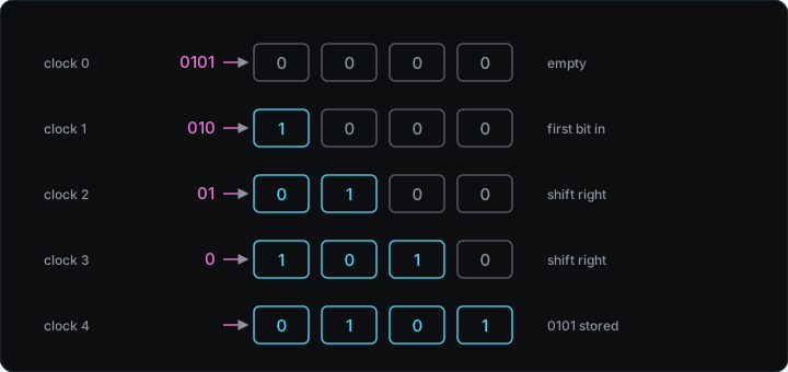
| Serial shift register | On each clock pulse, loads a new bit into the first cell and moves the stored bits one cell over |
| Parallel register | Stores several bits at once on a single clock pulse |
| Counter | Advances to the next binary number on each incoming pulse |
Joining a MUX and a DEMUX with one line lets the three data streams A, B and C pass in turn during the intervals $\Delta t_1$, $\Delta t_2$ and $\Delta t_3$, and the receiving side separates them in the same order onto D, E and F. The figure below shows 0101 entering a 4-bit serial shift register. Loading 4 bits takes 4 clock pulses, whereas a parallel register takes the same 4 bits in a single pulse.
As pulses 1, 2, 3, 4 and 5 arrive at a counter, its output changes to the binary codes for 1, 2, 3, 4 and 5. After 6 pulses the output is 110.
The tablet bottling system
Figure 1-28 of the textbook connects all of the blocks above into a system that fills each bottle with a preset number of tablets and accumulates the total20.
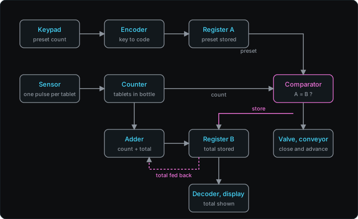
- The preset count is keyed in, the encoder converts it to a binary code, and register A stores it.
- Each tablet that drops produces one pulse from the sensor, and the counter advances by 1.
- The comparator compares the preset count in register A with the current count in the counter. When they match, the $A = B$ output goes HIGH.
- That HIGH goes to two places. It closes the valve and advances the conveyor, and at the same time it tells register B to store the new sum.
- The adder adds the counter value to the running total in register B, and register B stores the result as the new total. The decoder shows it on the display and the MUX sends it to a computer.
- When the next bottle is in place, a reset pulse returns the counter to zero.
The counter itself has no upper limit. It stops at the preset count because the closed valve cuts off the sensor pulses. Without the reset pulse the counter would run past the preset count on the second bottle, $A = B$ would never go HIGH again, and the valve would never close. The connection that returns the output of register B to the adder input is feedback21, and filling three bottles with a preset count of 8 updates register B to 8, 16 and 24.
Period, cycle, pulse and bit time
| Name | Meaning | Length |
|---|---|---|
| Period $T$ | Time for the waveform to repeat once | $T$ |
| Clock cycle | One repetition of the clock waveform | $T$ |
| Bit time | Time during which one data bit is held | $T$ |
| Pulse | The HIGH interval within a cycle | $t_W$ |
| Frequency $f$ | Number of cycles in one second | $1/T$, in Hz |
The first three are the same interval under different names. Each cycle contains exactly one pulse, so the counts agree while the lengths differ, with $t_W \le T$. A question about time is answered in seconds, a question about repetitions per second in Hz, and a question about a ratio with the duty cycle.
Exercise
For a system with a 2.5 GHz clock and a 25 % duty cycle, find the following.
(a) The clock period and the pulse width $t_W$ (b) The time to transfer 8 bits serially with this clock (c) The outputs of $\mathrm{AND}(A, C)$ and $\mathrm{OR}(B, C)$ in period 5 of the timing diagram above (d) The minimum number of output lines needed to encode a 16-key keypad (e) In the bottling system, the value of register B right after three bottles are filled with a preset count of 8, and the minimum number of bits needed to hold it
Solution. (a) $T = 1/(2.5 \times 10^9) = 0.4\ \mathrm{ns} = 400\ \mathrm{ps}$ and $t_W = 0.25\,T = 100\ \mathrm{ps}$. (b) The bit time is $T$, so the transfer takes $8T = 3.2\ \mathrm{ns}$. (c) In period 5, $(A, B, C) = (1, 0, 1)$, so $\mathrm{AND}(A, C) = 1$ and $\mathrm{OR}(B, C) = 1$. (d) $2^4 = 16$, so 4 lines. (e) $8 + 8 + 8 = 24$, and $2^4 = 16 \le 24 < 32 = 2^5$, so 5 bits.
Orientation
[19:44],[20:19]. The instructor split the keywords of the syllabus into “concepts of numbers, logic and formulas” and “the circuits that implement them”. The course covers Chapters 1 through 9, with one midterm, one final, and about four homework sets drawn mainly from the exercises. ↩︎Slide numbers are the printed numbers at the bottom of the lecture slides “Ch. 1. Introductory Concepts” (Kwangeun Kim, School of Electronics and Electrical Engineering, Hongik University). Timestamps
[MM:SS]refer to the transcript of the 2026-09-02 lecture recording, and those marked “orientation” refer to the transcript of the first class on 2026-09-01. ↩︎Lecture
[27:07]. The instructor described digital as “values distinguished as 0 and 1” and analog as “continuous values”, using the temperature over time sampled into digital form as the example. ↩︎Digital-to-Analog Converter, a circuit that turns a digital code into an analog voltage. In the CD player block diagram on slide 5, the digital data passes through the DAC on its way to the speaker. ↩︎
Lecture
[28:52]. The signal processing and communications courses treat this process as sampling and modulation. ↩︎Lecture
[31:25]. The charger receives AC and the battery stores DC, so a converter sits between them, and an inverter turns the DC back into AC to drive the motor. ↩︎Orientation
[29:54], lecture[07:06]. The chip handed out at the orientation was an SN74HC86N, with pin 14 as $V_{CC}$ and pin 7 as GND. The power supply keeps 5 V on that pin. ↩︎Lecture
[34:53],[35:54]. Once CPU clocks reach the GHz range the period is in ns and the rise time is a value below 1 ns, so it can no longer be ignored. The instructor put it as “a digital signal becomes analog when the time axis is viewed finely enough” and called it an item that matters in actual implementation. ↩︎Lecture
[37:08]. The instructor explained period and frequency as reciprocals with the examples 0.1 s and 10 Hz, and 1 GHz and 1 ns. ↩︎Slide 11 marks “Bit time” across the width of one clock period. This is the definition for the case of one bit per clock period, which is how Chapter 1 of this course always treats it. ↩︎
Lecture
[09:39],[25:25]. A function generator produces sine and square waves, and for a square wave the period, the ON time and the duty cycle are entered. Because the clock has a constant period, it is produced by the function generator in the laboratory. ↩︎Lecture
[24:41],[26:03],[38:26]. Values are read only where the clock coincides, and the output follows the same period. A, B and C are data that vary independently over time, and the clock cuts out the combination of the three values at fixed intervals. ↩︎Slide 13. The transcript contains no matching remark. ↩︎
Orientation
[43:09]. The instructor pointed out that the circle on a gate symbol is the NOT concept. ↩︎Orientation
[31:53],[36:40]. The 74HC86 handed out is an IC containing four 2-input XOR gates, and the logic circuit laboratory verifies truth tables directly with AND, OR and XOR chips. ↩︎Lecture
[40:58]. The instructor noted that the blocks come one slide each after the list of gates. ↩︎Slide 19 reads $3 + 9 = 12$ as a sum digit of 2 and a carry of 1. Adding directly in binary gives $0011 + 1001 = 1100$, with each digit producing one bit of $\Sigma$ and one carry bit. The rules of binary addition are covered in Chapter 2. ↩︎
A component that shows one digit with seven bars. At
[41:53]the instructor explained that choosing which of the seven bars to light produces the digit. ↩︎Orientation
[24:08]. Latches, flip-flops, registers and counters were set apart as “circuits that respond to data changing over time and thereby affect the result”. ↩︎Lecture
[42:47],[43:09]. Individual blocks are never used one at a time and are grouped for a purpose. The instructor went on to define engineering as “developing something out of the need for it to be used somewhere” and added that devices carrying people, such as electric vehicles and aircraft, have safety requirements on top. ↩︎A connection that returns an output to its own input. From Chapter 7 on, latches, flip-flops and counters hold their values with this structure. ↩︎